Reverse Engineering an ASIC
My write-up of the Jane Street 2026 "Can you reverse engineer an ASIC?" challenge, from the perspective of someone taking a crash course in VLSI along the way.
Toolkit code: github.com/jlvargasme/asic-2026-challenge — repo is being cleaned up; link is a placeholder for now.
I came across the Jane Street ASIC reverse engineering challenge on a LinkedIn post. Since college I have been exploring low-level programming and had a basic understanding of RTL and how chips work. However, I never went too deep into VLSI and how logic gates are physically laid out on a chip, so I thought it would be cool to learn.
The challenge gives you a chip .gds file, which contains the physical placement of the layers that make up the silicon. The goal is to figure out which input to the chip makes the success output line go high.
![puzzle.gds rendered as a connectivity graph, with input/clk/enable/rst_n entering on the left and out[0..7]/success leaving on the right](/assets/fig01.DfFyIugL.png)
Figure 1 — puzzle.gds as a network plot. Serial input, clk, enable and rst_n enter on the left; out[0..7] and success leave on the right. The shaded block near the outputs is the "output generator".
Jane Street also provided a warmup 04_final.gds file of a much smaller circuit, together with its Verilog source, to help get started.
My goal was a solution general enough to carry over from the 04_final.gds warmup to puzzle.gds with as few hand-tuned constants as possible. What follows is a summary of how I got there.
The target
Stripped of everything the GDS doesn't tell you, puzzle.gds has a small interface: a serial data input I, a clock clk, an enable, an active-low reset rst_n, an 8-bit output bus O[0..7], and a single success line.
module puzzle (
    input  I, clk, enable, rst_n,
    output O_0_, O_1_, O_2_, O_3_, O_4_, O_5_, O_6_, O_7_,
    output success
);
You clock a bit sequence in on I, one bit per cycle, and somewhere down the line success goes high — or doesn't. What the right sequence is, how long it is, and what the chip does with it all have to be recovered from reverse engineering.
Reverse engineering the warmup
Before touching puzzle.gds itself, I worked through Jane Street's warmup circuit, adder_demo, to build and sanity-check the whole reverse-engineering toolkit on something small enough to verify by eye.
adder_demo
My first instinct was to open the warmup GDS with the Tiny Tapeout GDS Viewer (linked from the challenge's GitHub repo).
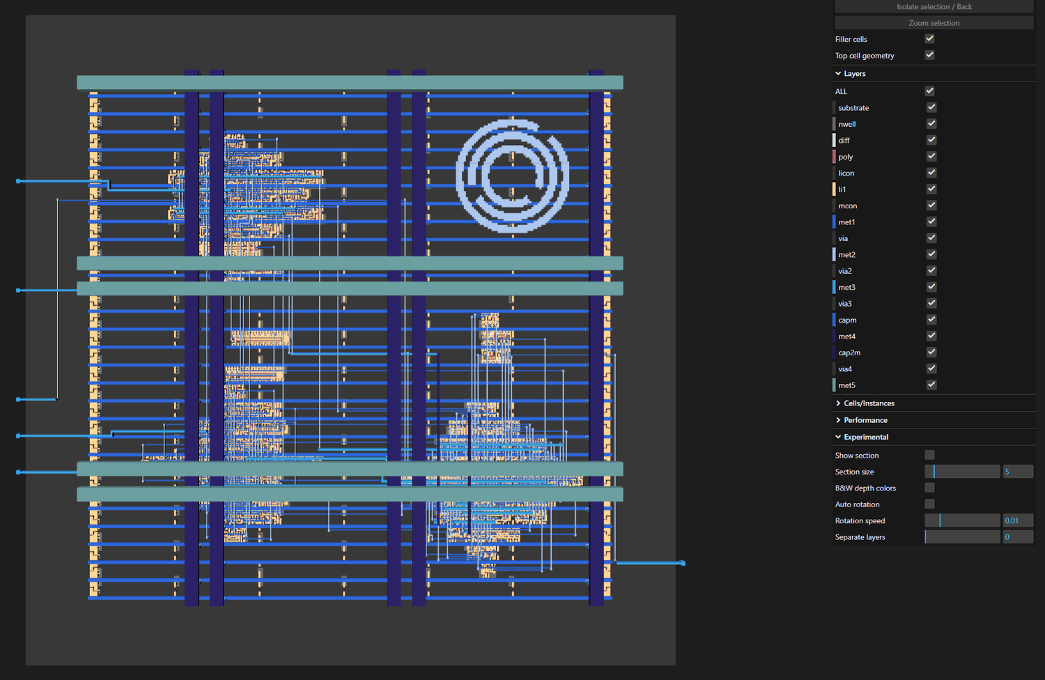
Figure 2 — Tiny Tapeout GDS Viewer showing the adder_demo cell list.
The cell tab showed descriptive names such as sky130_fd_sc_hd__and3_2 — clearly a 3-input AND gate. That seemed like a good place to start reverse engineering by hand, and to work out the general process of lifting a physical layout back up to logic gates.
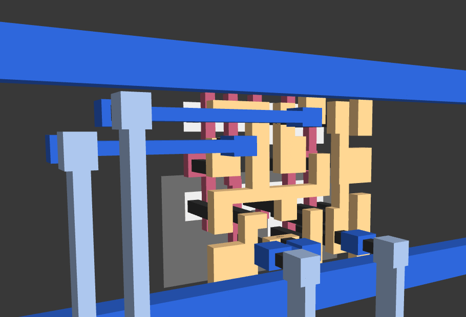
Figure 3 — The sky130_fd_sc_hd__and3_2 cell, as shown in the GDS viewer.
I knew logic gates were built from transistors, but not much about how a transistor is physically built. Fortunately I found an illustrative guide to VLSI electronics that helped me learn how to "see" a transistor.
The key idea from those notes: a transistor is created wherever a polysilicon (poly) wire crosses a diffusion (diff) region. So in the and3_2 cell (Figure 4), each red dot is a transistor.
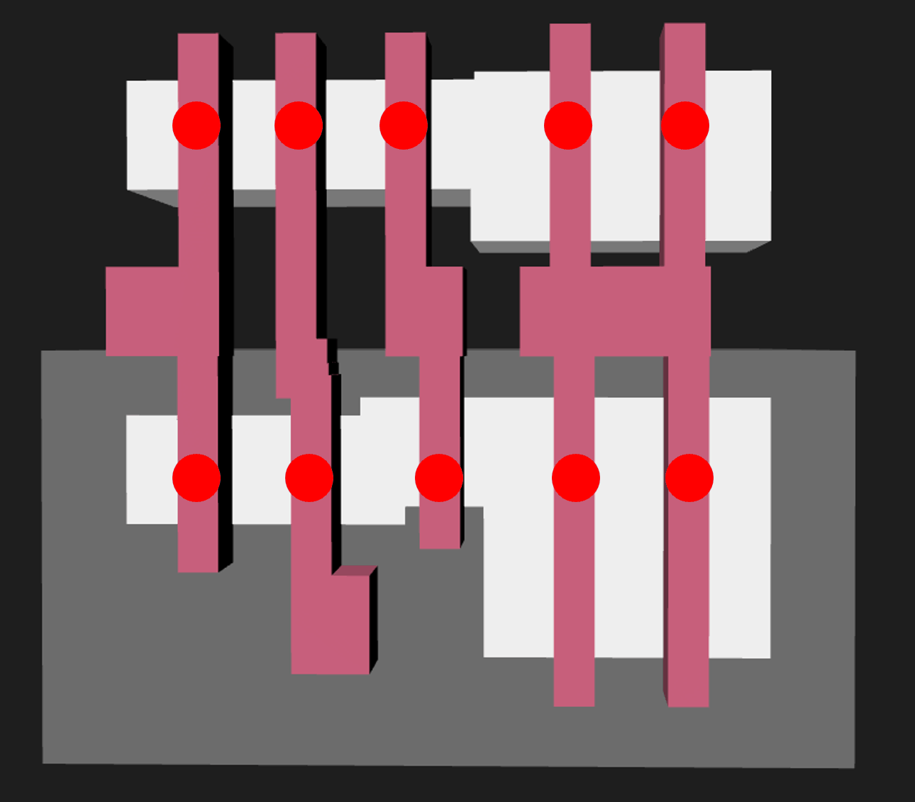
Figure 4 — sky130_fd_sc_hd__and3_2: poly, diff and nwell layers, with each poly/diff crossing (a transistor) marked in red.
I also spent time exploring the viewer to get familiar with what a GDS actually contains. In short: the GDS holds the 2D geometry of how the chip is laid out; the 3D information — the layer stack — is a separate standard that lives outside the file.
Looking up the layer names, puzzle.gds follows the Sky130 process design rules for its layer stack. Under Sky130, the substrate is the silicon itself, diff is the diffusion layer, poly the polysilicon, and most of the remaining layers are metal. li1 and met1–met5 are horizontal connections; licon, mcon and via1–via4 are vertical connections. The other interesting layer is nwell — a region doped with n-type impurities inside the p-type substrate, used to build a PMOS.
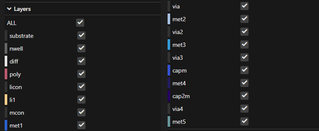
Figure 5 — Sky130 layer stack, toggled in the viewer's layer panel.
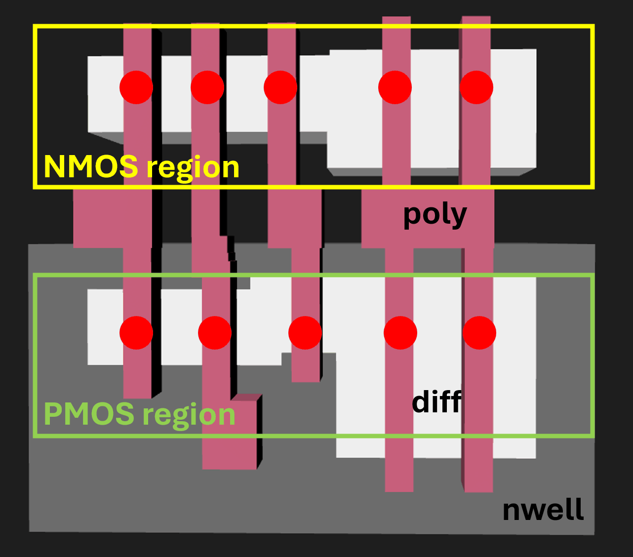
Figure 6 — NMOS region (plain diff) vs. PMOS region (diff inside nwell) in the and3 cell; each poly/diff crossing is a transistor (red dot).
In short: if an nwell surrounds a diff region that a poly crosses, that crossing is a PMOS. A poly crossing plain diff (no well) is an NMOS.
For the warmup I could actually read the gate type, inputs and output straight from the cell definition and its GDS metadata. sky130_fd_sc_hd__and3_2 is a 3-input AND with inputs labeled A, B, C and output X — enough to find connections to other cells and start building the logic. But that wouldn't work on a manufacturing file where cell and pin names are stripped or obfuscated, so I wanted a purely geometric approach.
Identifying and counting transistors in a cell was a good starting point. gdstk makes it easy to pull the polygons for a given layer and test for geometric intersection with a boolean operation.
poly = cell.get_polygons(depth=None, layer=layers.poly[0],
                         datatype=layers.poly[1])

diff = cell.get_polygons(depth=None, layer=layers.diff[0],
                         datatype=layers.diff[1])

nwell = cell.get_polygons(depth=None, layer=layers.nwell[0],
                          datatype=layers.nwell[1])

gates = gdstk.boolean(poly, diff, "and", precision=precision)
if min_area > 0:
    gates = [g for g in gates if g.area() >= min_area]

nmos = pmos = 0
for gate in gates:
    overlap = gdstk.boolean(gate, nwell, "and", precision=precision)
    overlap_area = sum(p.area() for p in overlap)
    if overlap_area == gate.area():
        pmos += 1
    else:
        nmos += 1
Figure 7 — Poly ∩ diff intersection locates the transistor gates; overlap with nwell classifies each as PMOS or NMOS.
=== ./warmup/04_final.gds :: sky130_fd_sc_hd__and3_2 ===

transistors found: 10  (nmos=5, pmos=5)
Figure 8 — Intersection result.
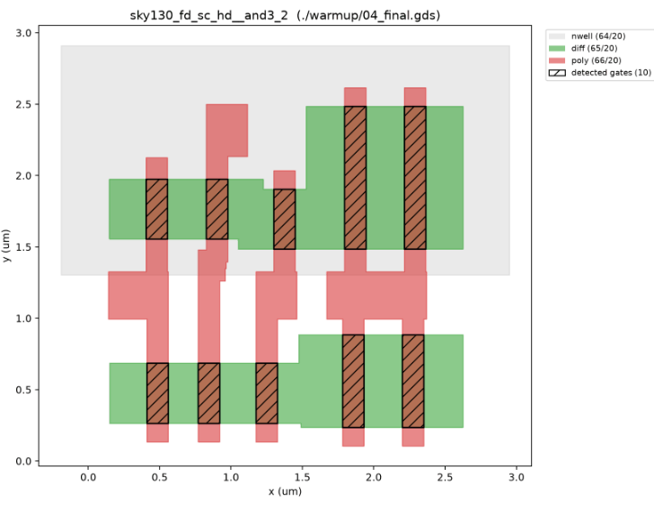
Figure 9 — The identified transistors in the and3_2 cell.
TIP
Note that the _2 in and3_2 stands for the drive strength, meaning that this gate is designed to drive twice the capacitive load compared to the baseline strength. This is why there are two sets of NMOS-PMOS transistors connected as the output.
Building a logic gate from geometry
The next step was to find the gate, source and drain terminals for each transistor. I did the first one by hand looking at the GDS, labeling each transistor N (NMOS) or P (PMOS), with A, B, C as inputs and X as output (Figure 10).
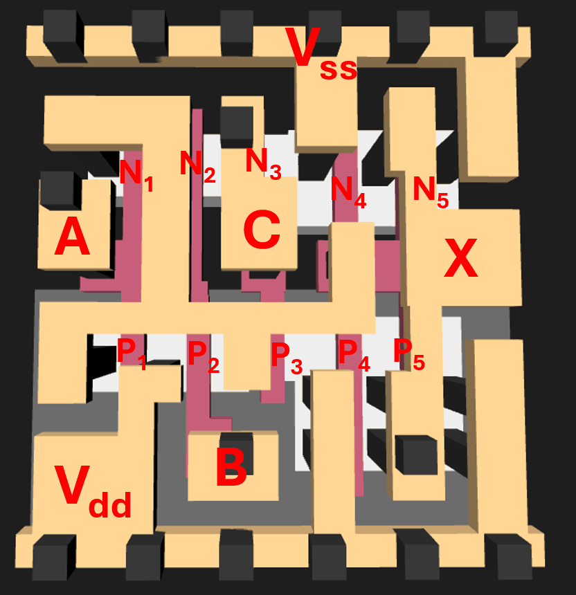
Figure 10 — The and3 cell with pins A/B/C/X/Vdd/Vss and all 10 transistors (N1–N5, P1–P5) labeled by hand.
Tracing the connections by eye, I sketched the transistor-level schematic (Figure 11). Doing it manually gave me the shape of the algorithm: first trace the metal connections, then decide which nets are inputs and which are outputs.
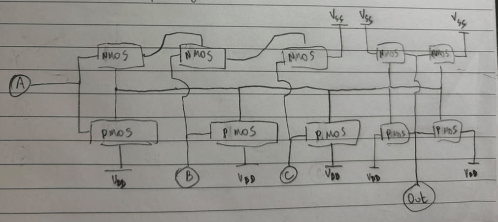
Figure 11 — Hand-drawn transistor-level schematic of the and3 cell, reconstructed from the labeled connections.
To trace connections, the idea is to find which layers overlap or have touching edges (Figure 12). The fixed layer ordering in Sky130 lets this traversal walk the cell structure and recover the full metal connectivity.
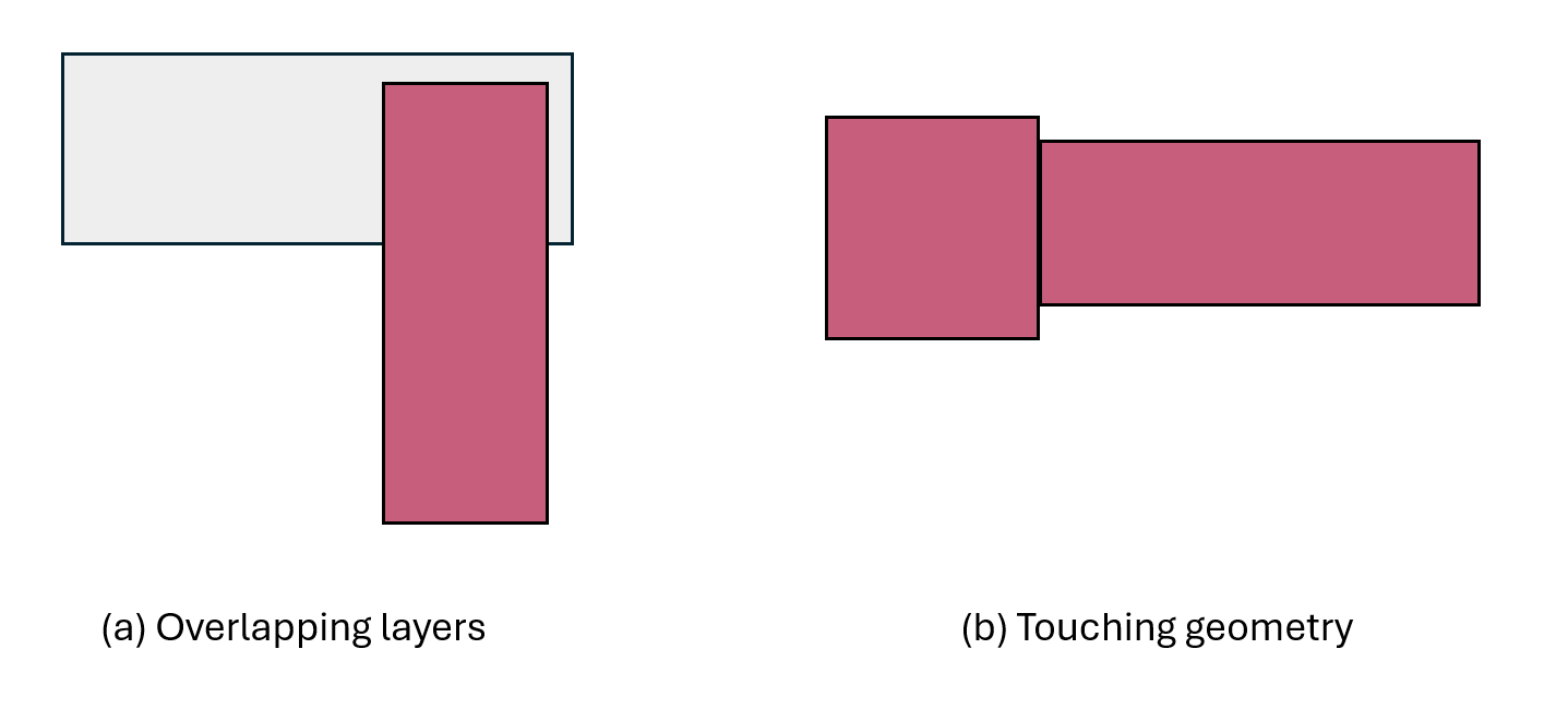
Figure 12 — The two geometric connectivity cases traced between layers: overlapping regions (a) and edge-touching regions (b).
The missing piece was a way to name the intermediate diffusion nodes that are neither input nor output. I did this by partitioning the diffusion layer: remove the transistor-gate regions, then label whatever is left. I used DN_i (diff, NMOS side) and DP_i (diff, PMOS side), as in Figure 13. Each transistor then touches exactly two of these regions, arbitrarily assigned as source and drain.
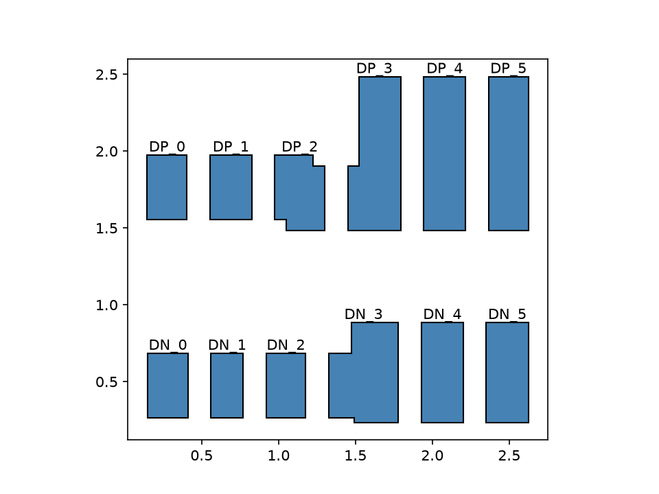
Figure 13 — Diffusion layer partitioned into DN_i/DP_i regions after removing the transistor gates.
transistors:
  gate=GP_0     kind=TransistorType.PMOS source=DP_3 drain=DP_4
  gate=GP_1     kind=TransistorType.PMOS source=DP_4 drain=DP_5
  gate=GP_2     kind=TransistorType.PMOS source=DP_0 drain=DP_1
  gate=GP_3     kind=TransistorType.PMOS source=DP_1 drain=DP_2
  gate=GP_4     kind=TransistorType.PMOS source=DP_2 drain=DP_3
  gate=GN_5     kind=TransistorType.NMOS source=DN_3 drain=DN_4
  gate=GN_6     kind=TransistorType.NMOS source=DN_4 drain=DN_5
  gate=GN_7     kind=TransistorType.NMOS source=DN_2 drain=DN_3
  gate=GN_8     kind=TransistorType.NMOS source=DN_1 drain=DN_2
  gate=GN_9     kind=TransistorType.NMOS source=DN_0 drain=DN_1
Figure 14 — Extracted transistor list (gate / source / drain) using the DN_i/DP_i labeling.
With the structure in place, I wrote a NetTracer class that uses a union-find to track which labels are electrically connected. Each cell is a set of transistors whose gate, source and drain terminals share one namespace.
def connect(polys_a, keys_a, polys_b, keys_b):
  for pa, ka in zip(polys_a, keys_a):
    for pb, kb in zip(polys_b, keys_b):
      if _overlaps(pa, pb):
         self._uf.union(ka, kb)

def connect_self(polys, keys):
    """Union every pair of same-layer `polys` that either area-
    overlap or abut edge-to-edge -- see module docstring for why
    both checks are needed and why this is always safe."""
    for i in range(len(polys)):
       for j in range(i + 1, len(polys)):
          if _overlaps(polys[i], polys[j]) or _touching(polys[i], polys[j]):
             self._uf.union(keys[i], keys[j])

connect(diff_polys, diff_keys, licon, licon_keys)
connect(licon, licon_keys, li1, li1_keys)
connect_self(li1, li1_keys)
connect(li1, li1_keys, mcon, mcon_keys)
connect(mcon, mcon_keys, met1, met1_keys)
connect_self(met1, met1_keys)
connect(licon, licon_keys, poly, poly_keys)
connect_self(poly, poly_keys)
connect(poly, poly_keys, transistor_poly, transistor_keys)
Figure 15 — NetTracer's connect() / connect_self(), merging same-layer regions that overlap or touch via union-find.
This was good at finding connections inside a cell, but it couldn't tell which labeled regions were inputs or outputs, nor which were tied to power (Vdd/Vss). Transistor physics helps here. A transistor gate (poly) draws no DC current — it's capacitive — so the only reason a net would terminate there is that something outside drives it: that's an input. A source/drain diffusion node that isn't already tied to VPWR/VGND is the low-impedance node a pull-up/pull-down stage pushes current onto: that's an output.
touches_gate = any(e.startswith("G") for e in equivalents)  # GN_i / GP_i
touches_diff = any(e.startswith("D") for e in equivalents)  # DN_i / DP_i

if touches_gate and touches_diff:
   return "ambiguous"  # touches both a gate and a drain
if touches_gate:
   return "input"
if touches_diff:
   return "output"
return "unknown"  # isolated from the transistor graph entirely
Figure 16 — Deciding input vs. output per net: a net touching only a transistor gate is an input; one touching a diffusion node is an output.
Identifying power was more ad hoc: first check for explicit power labels (VPWR, VGND, VDD, VSS, GND); as a fallback, if unresolved polygons remain, guess by Euclidean distance to an nwell. That fallback comes from noticing that cells are usually split into an upper half tied to one rail and a lower half tied to the other.
With an arbitrary cell now decoded into transistors, inputs and outputs, I could plot its schematic (Figures 17–18) and reason about the logic in 2D instead of tracing the layout by hand.
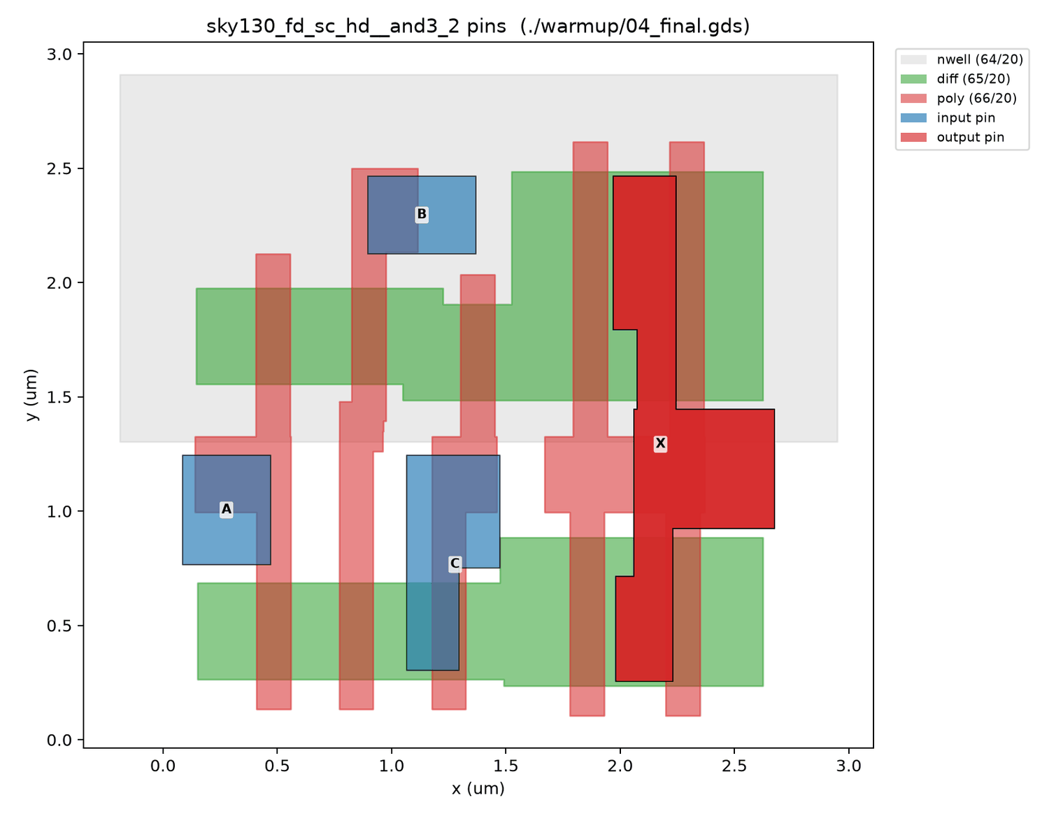
Figure 17 — Auto-detected input (A/B/C) and output (X) pins for the and3 cell, on the GDS geometry.
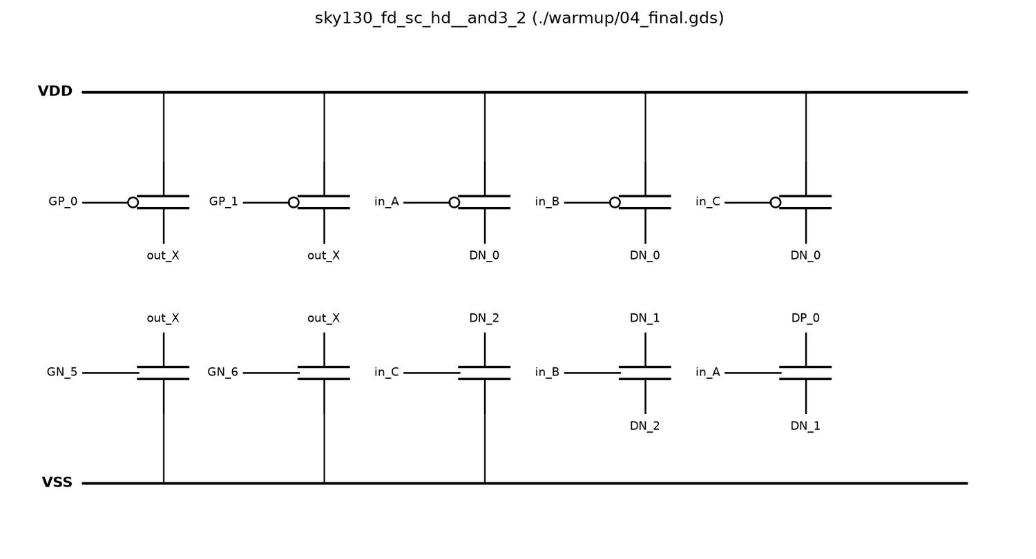
Figure 18 — Auto-generated transistor-level schematic of the and3 cell: PMOS row tied to VDD, NMOS row tied to VSS.
Simulating the cell (Z3 and PySpice)
The next step was going from the cell abstraction to its logic function. Rather than pattern-matching each cell to a named gate, I kept the cell abstraction as-is and simulated it — two ways: PySpice for the circuit physics, and Z3 for the pure logic.
SPICE simulation
SPICE numerically solves for the output voltage state. To build a transistor in PySpice you pick the model (NMOS or PMOS), give the device dimensions (read from the GDS), and name the gate/source/drain nets. Since labels are already resolved into the cell namespace, the circuit is just an iteration over the transistor objects.
if transistor.kind == TransistorType.NMOS:
     model, default_bulk = nmos_model, "VSS"
elif transistor.kind == TransistorType.PMOS:
     model, default_bulk = pmos_model, "VDD"
else:
    raise ValueError(f"transistor {transistor.gate_label} has no resolved NMOS/PMOS kind")

dims = _gate_dimensions(transistor)
if dims is not None:
    length, width = dims

return circuit.MOSFET(
    name if name is not None else transistor.gate_label,
    drain_net, gate_net, source_net, bulk_net or default_bulk,
    model=model, l=length, w=width,
)
Figure 19 — PySpice transistor-level circuit built from the extracted cell geometry.
Z3 simulation
Z3 is an SMT solver: given constraints over a set of variables, it finds an assignment that satisfies them all. Encoding a transistor as logic:
- NMOS:
G ⇒ (S == D)— conducts (source and drain equal) when the gate is high. - PMOS:
¬G ⇒ (S == D)— conducts when the gate is low.
if transistor.kind == TransistorType.NMOS:
    condition = gate_var
elif transistor.kind == TransistorType.PMOS:
    condition = z3.Not(gate_var)
else:
    raise ValueError(f"transistor {transistor.gate_label} has no resolved NMOS/PMOS kind")

return z3.Implies(condition, source_var == drain_var)
Figure 20 — Z3 encoding of a transistor: NMOS conducts when gate = 1, PMOS when gate = 0, both as source == drain.
A bonus of the Z3 encoding is that I can search for input assignments that produce a specific output — e.g. add the constraint OutX == 1 and ask for a model. If several input combinations drive the output high, I can enumerate them: solve, block that exact assignment, solve again, and repeat until it comes back unsat.
solver = z3.Solver()
solver.add(self.z3_circuit)
solver.add(self.z3_outputs[output_label] == bool(target))

input_vars = [self.z3_inputs[name] for name in self.input_labels]
solutions = []
while solver.check() == z3.sat:
     model = solver.model()
     values = tuple(
         int(z3.is_true(model.eval(v, model_completion=True)))
         for v in input_vars
     )
     solutions.append(values)
     # block this exact input combination so the next check() is
     # forced to either find a different one or come back unsat
     solver.add(
      z3.Or([v != z3.BoolVal(bool(val)) for v, val in zip(input_vars, values)]))

return solutions
Figure 21 — Enumerating every input combination that drives a target output, blocking each solution before the next solve.
sky130_fd_sc_hd__and3_2: inputs=['A', 'B', 'C'] outputs=['X']
PySpice simulation:
  {'A': 0, 'B': 0, 'C': 0} -> [0]
  {'A': 0, 'B': 0, 'C': 1} -> [0]
  {'A': 0, 'B': 1, 'C': 0} -> [0]
  {'A': 0, 'B': 1, 'C': 1} -> [0]
  {'A': 1, 'B': 0, 'C': 0} -> [0]
  {'A': 1, 'B': 0, 'C': 1} -> [0]
  {'A': 1, 'B': 1, 'C': 0} -> [0]
  {'A': 1, 'B': 1, 'C': 1} -> [1]
Z3 simulation:
  {'A': 0, 'B': 0, 'C': 0} -> [0]
  {'A': 0, 'B': 0, 'C': 1} -> [0]
  {'A': 0, 'B': 1, 'C': 0} -> [0]
  {'A': 0, 'B': 1, 'C': 1} -> [0]
  {'A': 1, 'B': 0, 'C': 0} -> [0]
  {'A': 1, 'B': 0, 'C': 1} -> [0]
  {'A': 1, 'B': 1, 'C': 0} -> [0]
  {'A': 1, 'B': 1, 'C': 1} -> [1]
Search for inputs that satisfy the gate: -> {'A': in_A, 'B': in_B, 'C': in_C}:[(1, 1, 1)]
Figure 22 — PySpice and Z3 truth tables for the and3 cell agree on every input, including the one that drives X high.
From one cell to N: building a chip
At this point I could take any cell in the GDS, recover its transistor connections from geometry, and simulate the gate with Z3 or PySpice.
Next I had to wire the cells together into a chip-level netlist. Using adder_demo, I checked each cell independently to confirm:
- Z3 and PySpice agreed.
- Z3 matched the logic implied by the Sky130 cell name.
That shook out a few bugs and surfaced cells that didn't fit the toolkit:
sky130_fd_sc_hd__clkbuf_16— a clock buffer introduced by synthesis, not present in the source Verilog.sky130_fd_sc_hd__dfrtp_2— a CMOS D flip-flop; it breaks the pure-combinational Z3 model by feeding logic back on itself.sky130_fd_sc_hd__decap_3— decoupling capacitors; a physical artifact to prevent latch-up, not a logic gate.sky130_fd_sc_hd__tapvpwrvgnd_1— a well/substrate tap; like decap, not a logic cell.
The other problem in connecting cells is that the per-cell namespace isn't unique, so I built a global chip namespace (again union-find, preferring GDS labels where present) to resolve inter-cell connectivity.
Determining the chip's own inputs and outputs needed a bit more: first keep only nets that cross the chip's footprint boundary — a purely internal wire can never be a port — then label those by whether they're driven.
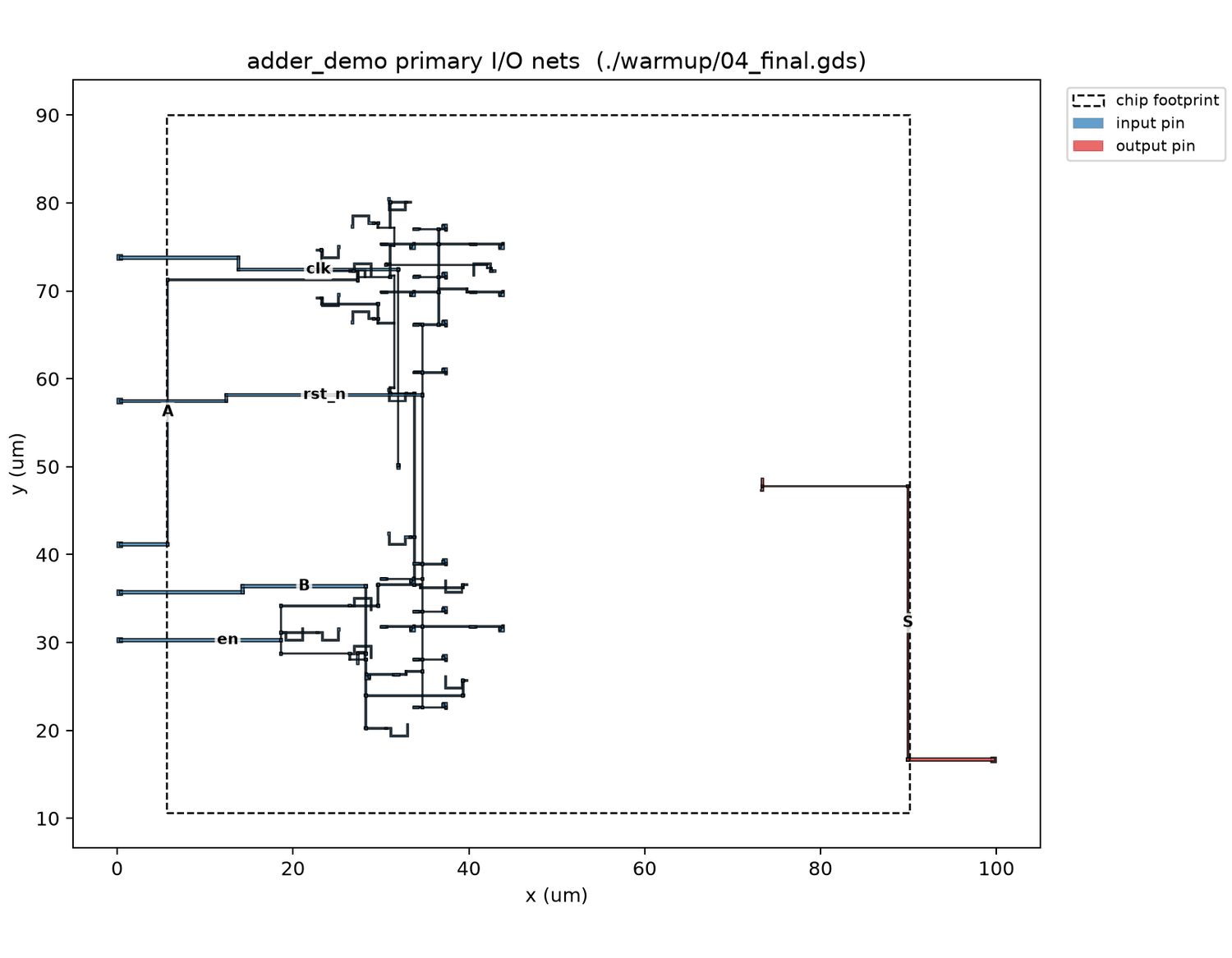
Figure 23 — adder_demo's primary I/O nets, detected by which wires cross the chip's footprint boundary.
Understanding the chip
With the chip wired into one netlist, the next problem was scale: a flat graph of hundreds of gates isn't something you can reason about directly. Comparing the source to the layout, I noticed each Verilog module mapped to a physical cluster of cells. So I grouped cells by a simple heuristic: measure the edge-to-edge distance between two cells, and if it's smaller than the cell's own smallest dimension, put them in the same cluster.
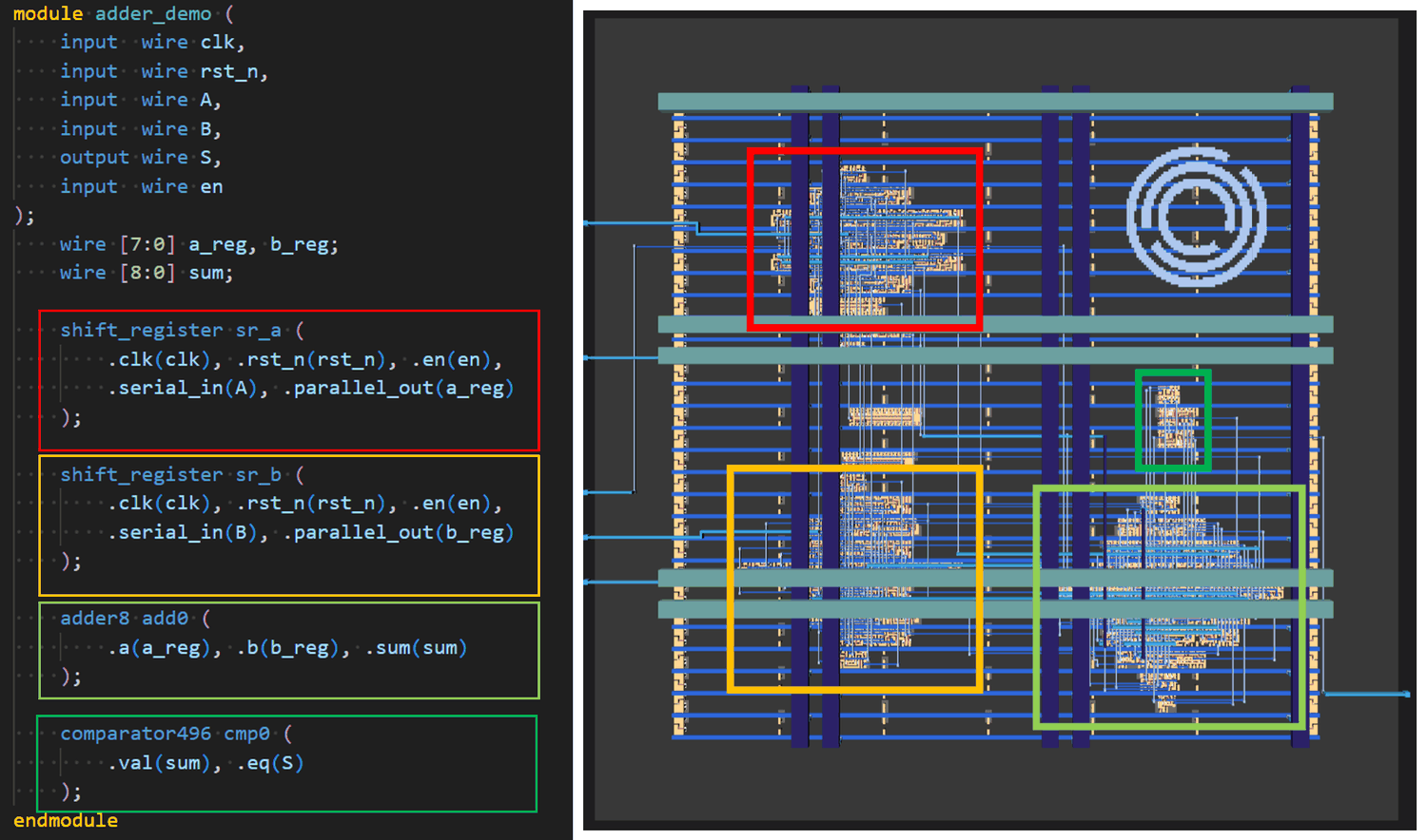
Figure 24 — adder_demo's source modules (left) color-matched to the physical cell clusters they map to (right).
Because adder_demo is small, I could convert every combinational cluster to Z3 and treat the sequential clusters as free inputs. That was enough constraint to solve for all fifteen input/register assignments that drive adder_demo's success high.
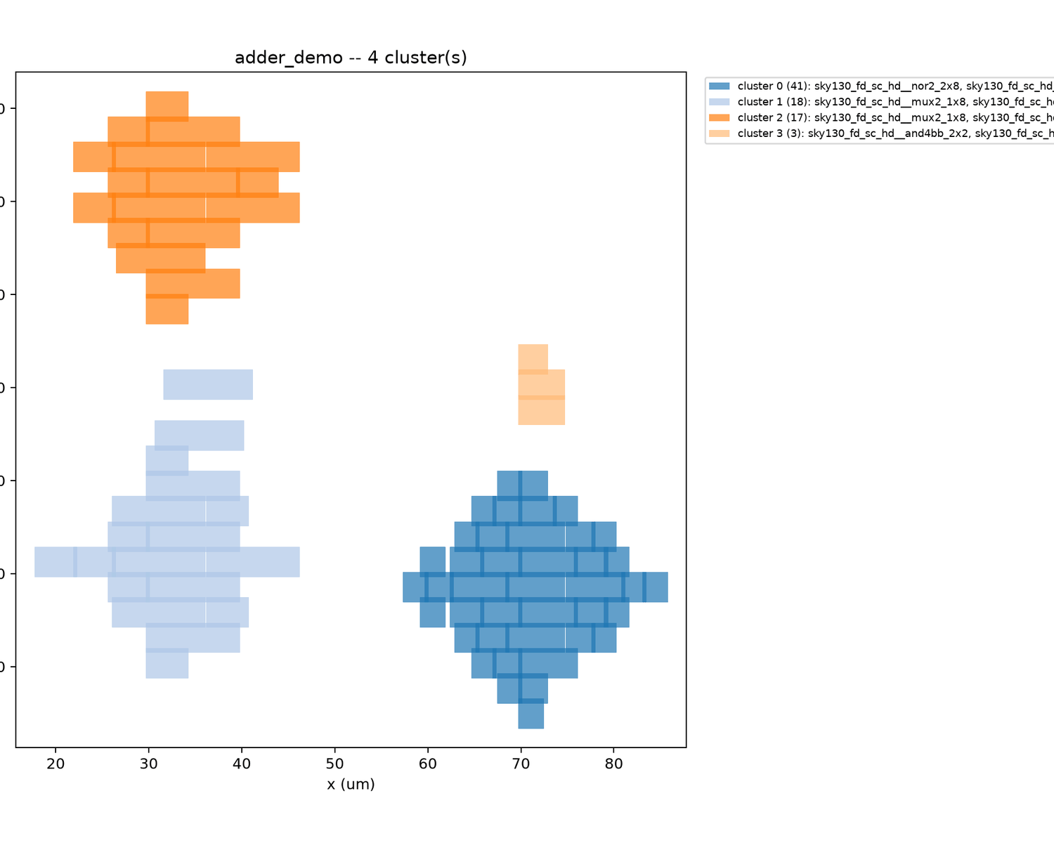
Figure 25 — adder_demo's cells auto-grouped into 4 clusters by the edge-to-edge distance heuristic.
solving for all 1 output net(s) == 1: ['S']

16 free net(s) (chip primary inputs + sequential-cluster/register state -- see build_chip_z3_circuit's docstring): ['B#5', 'B#2', 'B#1', 'B#0', 'B#6', 'B#3', 'B#7', 'B#4', 'A#3', 'A#2', 'A#4', 'A#6', 'A#5', 'A#0', 'A#1', 'A#7']
15 assignment(s) drive every output net to 1:

{'B#5': 1, 'B#2': 0, 'B#1': 0, 'B#0': 0, 'B#6': 1, 'B#3': 1, 'B#7': 1, 'B#4': 1, 'A#3': 1, 'A#2': 0, 'A#4': 1, 'A#6': 1, 'A#5': 1, 'A#0': 0, 'A#1': 0, 'A#7': 1}
  -> A=11111000 (248), B=11111000 (248)  sum=496  == 496 OK
{'B#5': 1, 'B#2': 0, 'B#1': 1, 'B#0': 1, 'B#6': 1, 'B#3': 0, 'B#7': 1, 'B#4': 1, 'A#3': 1, 'A#2': 1, 'A#4': 1, 'A#6': 1, 'A#5': 1, 'A#0': 1, 'A#1': 0, 'A#7': 1}
  -> A=11111101 (253), B=11110011 (243)  sum=496  == 496 OK
{'B#5': 1, 'B#2': 0, 'B#1': 1, 'B#0': 1, 'B#6': 1, 'B#3': 1, 'B#7': 1, 'B#4': 1, 'A#3': 0, 'A#2': 1, 'A#4': 1, 'A#6': 1, 'A#5': 1, 'A#0': 1, 'A#1': 0, 'A#7': 1}
  -> A=11110101 (245), B=11111011 (251)  sum=496  == 496 OK
{'B#5': 1, 'B#2': 1, 'B#1': 1, 'B#0': 1, 'B#6': 1, 'B#3': 1, 'B#7': 1, 'B#4': 1, 'A#3': 0, 'A#2': 0, 'A#4': 1, 'A#6': 1, 'A#5': 1, 'A#0': 1, 'A#1': 0, 'A#7': 1}
  -> A=11110001 (241), B=11111111 (255)  sum=496  == 496 OK
{'B#5': 1, 'B#2': 1, 'B#1': 1, 'B#0': 1, 'B#6': 1, 'B#3': 0, 'B#7': 1, 'B#4': 1, 'A#3': 1, 'A#2': 0, 'A#4': 1, 'A#6': 1, 'A#5': 1, 'A#0': 1, 'A#1': 0, 'A#7': 1}
  -> A=11111001 (249), B=11110111 (247)  sum=496  == 496 OK
{'B#5': 1, 'B#2': 1, 'B#1': 0, 'B#0': 0, 'B#6': 1, 'B#3': 1, 'B#7': 1, 'B#4': 1, 'A#3': 0, 'A#2': 1, 'A#4': 1, 'A#6': 1, 'A#5': 1, 'A#0': 0, 'A#1': 0, 'A#7': 1}
  -> A=11110100 (244), B=11111100 (252)  sum=496  == 496 OK
{'B#5': 1, 'B#2': 1, 'B#1': 0, 'B#0': 0, 'B#6': 1, 'B#3': 0, 'B#7': 1, 'B#4': 1, 'A#3': 1, 'A#2': 1, 'A#4': 1, 'A#6': 1, 'A#5': 1, 'A#0': 0, 'A#1': 0, 'A#7': 1}
  -> A=11111100 (252), B=11110100 (244)  sum=496  == 496 OK
{'B#5': 1, 'B#2': 0, 'B#1': 0, 'B#0': 1, 'B#6': 1, 'B#3': 1, 'B#7': 1, 'B#4': 1, 'A#3': 0, 'A#2': 1, 'A#4': 1, 'A#6': 1, 'A#5': 1, 'A#0': 1, 'A#1': 1, 'A#7': 1}
  -> A=11110111 (247), B=11111001 (249)  sum=496  == 496 OK
{'B#5': 1, 'B#2': 0, 'B#1': 0, 'B#0': 1, 'B#6': 1, 'B#3': 0, 'B#7': 1, 'B#4': 1, 'A#3': 1, 'A#2': 1, 'A#4': 1, 'A#6': 1, 'A#5': 1, 'A#0': 1, 'A#1': 1, 'A#7': 1}
  -> A=11111111 (255), B=11110001 (241)  sum=496  == 496 OK
{'B#5': 1, 'B#2': 1, 'B#1': 0, 'B#0': 1, 'B#6': 1, 'B#3': 0, 'B#7': 1, 'B#4': 1, 'A#3': 1, 'A#2': 0, 'A#4': 1, 'A#6': 1, 'A#5': 1, 'A#0': 1, 'A#1': 1, 'A#7': 1}
  -> A=11111011 (251), B=11110101 (245)  sum=496  == 496 OK
{'B#5': 1, 'B#2': 1, 'B#1': 0, 'B#0': 1, 'B#6': 1, 'B#3': 1, 'B#7': 1, 'B#4': 1, 'A#3': 0, 'A#2': 0, 'A#4': 1, 'A#6': 1, 'A#5': 1, 'A#0': 1, 'A#1': 1, 'A#7': 1}
  -> A=11110011 (243), B=11111101 (253)  sum=496  == 496 OK
{'B#5': 1, 'B#2': 1, 'B#1': 1, 'B#0': 0, 'B#6': 1, 'B#3': 0, 'B#7': 1, 'B#4': 1, 'A#3': 1, 'A#2': 0, 'A#4': 1, 'A#6': 1, 'A#5': 1, 'A#0': 0, 'A#1': 1, 'A#7': 1}
  -> A=11111010 (250), B=11110110 (246)  sum=496  == 496 OK
{'B#5': 1, 'B#2': 0, 'B#1': 1, 'B#0': 0, 'B#6': 1, 'B#3': 0, 'B#7': 1, 'B#4': 1, 'A#3': 1, 'A#2': 1, 'A#4': 1, 'A#6': 1, 'A#5': 1, 'A#0': 0, 'A#1': 1, 'A#7': 1}
  -> A=11111110 (254), B=11110010 (242)  sum=496  == 496 OK
{'B#5': 1, 'B#2': 1, 'B#1': 1, 'B#0': 0, 'B#6': 1, 'B#3': 1, 'B#7': 1, 'B#4': 1, 'A#3': 0, 'A#2': 0, 'A#4': 1, 'A#6': 1, 'A#5': 1, 'A#0': 0, 'A#1': 1, 'A#7': 1}
  -> A=11110010 (242), B=11111110 (254)  sum=496  == 496 OK
{'B#5': 1, 'B#2': 0, 'B#1': 1, 'B#0': 0, 'B#6': 1, 'B#3': 1, 'B#7': 1, 'B#4': 1, 'A#3': 0, 'A#2': 1, 'A#4': 1, 'A#6': 1, 'A#5': 1, 'A#0': 0, 'A#1': 1, 'A#7': 1}
  -> A=11110110 (246), B=11111010 (250)  sum=496  == 496 OK
Figure 26 — The fifteen register/input assignments the Z3 model finds that drive adder_demo's S output high.
Decompiling the GDS
Clustering gave me a graph with module-shaped boundaries, but a graph still isn't code. So I went one step further: treat each cluster as a node in a Verilog AST and reconstruct source from it. I asked Claude to build a compiler that walked the AST and emitted Verilog; a couple of passes had to be added — clock-buffer removal and duplicate-cluster detection — before the output was readable.
The top-level module comes out close to the original source:
// Auto-generated by decompiler.py from adder_demo -- do not hand-edit.
module adder_demo (
    input A,
    input B,
    input clk,
    input en,
    input rst_n,
    output S
);
    wire [7:0] A_10_bus;
    wire [7:0] A0_bus;
    wire [8:0] A_2_bus;
    cluster_type_1 cluster_type_1_i0 (.A_10_bus(A_10_bus), .A0_4_bus(A0_bus), .A_2_bus(A_2_bus));
    cluster_type_0 cluster_type_0_i1 (.B(B), .clk(clk), .en(en), .rst_n(rst_n), .A_10_bus(A_10_bus));
    cluster_type_0 cluster_type_0_i2 (.B(A), .clk(clk), .en(en), .rst_n(rst_n), .A_10_bus(A0_bus));
    cluster_type_2 cluster_type_2_i3 (.A_2_bus(A_2_bus), .S(S));
endmodule
Listing 1 — The decompiled top-level adder_demo: the two shift registers reduced to two cluster_type_0 instances, the adder to cluster_type_1, the comparator to cluster_type_2.
The internal modules are more obfuscated, as expected when working backward from a synthesized, placed-and-routed layout. The decompiled cluster_type_0 is fully flattened combinational logic wired straight to individual flip-flops (sky130_fd_sc_hd__dfrtp_2 is the library D flip-flop):
// Auto-generated by decompiler.py from adder_demo -- do not hand-edit.

module sky130_fd_sc_hd__dfrtp_2 (
    input CLK,
    input D,
    input RESET_B,
    output reg Q
);
    // tier1(known-cell)
    always @(posedge CLK or negedge RESET_B) begin
        if (!RESET_B) begin
            Q <= 1'b0;
        end
        else begin
            Q <= D;
        end
    end
endmodule

module cluster_type_0 (
    input B,
    input clk,
    input en,
    input rst_n,
    output [7:0] A_10_bus
);
    wire D_10; wire D_11; wire D_12; wire D_13;
    wire D_14; wire D_15; wire D_16; wire D_17;
    // combinational logic flattened via z3 (see chip_manipulation.py)
    assign D_13 = (A_10_bus[4] & ~en) | (A_10_bus[0] & en);
    assign D_14 = (A_10_bus[5] & ~en) | (A_10_bus[1] & en);
    assign D_15 = (A_10_bus[6] & ~en) | (A_10_bus[4] & en);
    assign D_10 = (A_10_bus[1] & ~en) | (A_10_bus[2] & en);
    assign D_11 = (A_10_bus[2] & ~en) | (A_10_bus[3] & en);
    assign D_17 = (A_10_bus[0] & ~en) | (A_10_bus[7] & en);
    assign D_12 = (A_10_bus[3] & ~en) | (B & en);
    assign D_16 = (A_10_bus[7] & ~en) | (A_10_bus[5] & en);
    sky130_fd_sc_hd__dfrtp_2 sky130_fd_sc_hd__dfrtp_2_i3  (.CLK(clk), .D(D_13), .RESET_B(rst_n), .Q(A_10_bus[4]));
    sky130_fd_sc_hd__dfrtp_2 sky130_fd_sc_hd__dfrtp_2_i4  (.CLK(clk), .D(D_14), .RESET_B(rst_n), .Q(A_10_bus[5]));
    sky130_fd_sc_hd__dfrtp_2 sky130_fd_sc_hd__dfrtp_2_i5  (.CLK(clk), .D(D_15), .RESET_B(rst_n), .Q(A_10_bus[6]));
    sky130_fd_sc_hd__dfrtp_2 sky130_fd_sc_hd__dfrtp_2_i6  (.CLK(clk), .D(D_10), .RESET_B(rst_n), .Q(A_10_bus[1]));
    sky130_fd_sc_hd__dfrtp_2 sky130_fd_sc_hd__dfrtp_2_i10 (.CLK(clk), .D(D_11), .RESET_B(rst_n), .Q(A_10_bus[2]));
    sky130_fd_sc_hd__dfrtp_2 sky130_fd_sc_hd__dfrtp_2_i11 (.CLK(clk), .D(D_17), .RESET_B(rst_n), .Q(A_10_bus[0]));
    sky130_fd_sc_hd__dfrtp_2 sky130_fd_sc_hd__dfrtp_2_i12 (.CLK(clk), .D(D_12), .RESET_B(rst_n), .Q(A_10_bus[3]));
    sky130_fd_sc_hd__dfrtp_2 sky130_fd_sc_hd__dfrtp_2_i13 (.CLK(clk), .D(D_16), .RESET_B(rst_n), .Q(A_10_bus[7]));
endmodule
Listing 2 — Decompiled cluster_type_0. The (x & ~en) | (y & en) pattern on every D_* is a 2:1 mux — load vs. shift — but nothing about the flattened form says "shift register".
Compare adder_demo's own source, where the same behavior is one obvious module:
module shift_register (
    input  wire       clk,
    input  wire       rst_n,
    input  wire       en,
    input  wire       serial_in,
    output reg  [7:0] parallel_out
);
    always @(posedge clk or negedge rst_n) begin
        if (!rst_n)
            parallel_out <= 8'b0;
        else if (en)
            parallel_out <= {parallel_out[6:0], serial_in};
    end
endmodule
Listing 3 — The hand-written shift_register from adder_demo's source: the same behavior as Listing 2, far more readable.
As a last check on the warmup, I compiled the decompiled Verilog with Verilator and simulated it against arbitrary inputs. It matched the original — the whole pipeline, from GDS geometry to a working Verilog model, held end to end on a circuit small enough to still read by eye. Time to point it at the real target.
=== source: warmup/00_source.v ===
A=248 B=248 sum=496  expected S=1  actual S=1  -> PASS
A=100 B=100 sum=200  expected S=0  actual S=0  -> PASS
A=255 B=241 sum=496  expected S=1  actual S=1  -> PASS
A=  0 B=  0 sum=  0  expected S=0  actual S=0  -> PASS
A=255 B=255 sum=510  expected S=0  actual S=0  -> PASS
ALL CASES PASSED
wrote adder_demo_source.vcd

=== decompiled: adder_demo.v ===
A=248 B=248 sum=496  expected S=1  actual S=1  -> PASS
A=100 B=100 sum=200  expected S=0  actual S=0  -> PASS
A=255 B=241 sum=496  expected S=1  actual S=1  -> PASS
A=  0 B=  0 sum=  0  expected S=0  actual S=0  -> PASS
A=255 B=255 sum=510  expected S=0  actual S=0  -> PASS
ALL CASES PASSED
wrote adder_demo_decompiled.vcd
Using the toolkit on puzzle.gds
Testing the toolkit
Run on puzzle.gds, the toolkit held up reasonably well. A few new warnings showed up, mostly from cell types I hadn't handled: more flip-flop variants (sky130_fd_sc_hd__dfxtp_2, dfstp_2, dfrtp_2), a constant driver (sky130_fd_sc_hd__conb_1), more clock buffers, and a diode cell.
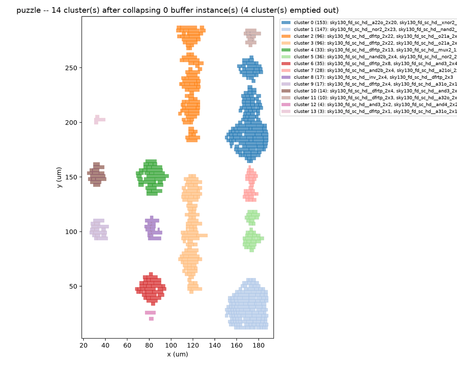
Figure 30 — puzzle.gds clustered into 14 groups by the same distance heuristic, after fixing a few bugs.
I also fed the sample .vcd into the synthesized Verilog to confirm the outputs matched. And this help clean-up some dangling internal wires.
Then puzzle.gds broke the one assumption the whole adder_demo flow rested on: that the circuit is small enough to flatten into a single Z3 model with registers as free inputs. Here that produced nonsense or nothing at all. The automated path was dead — the last stretch would have to be done by hand.
Reverse engineering the chip
With the Z3 pipeline out, I started reading the decompiled Verilog cluster by cluster and rebuilding an understanding of the chip from the bottom up.
It had thirteen clusters plus a top-level module. Reading them one by one was slow and not very illuminating on its own, but clues accumulated. For example, cluster8 and cluster9 are mod-11 4-bit counters — cluster9 the low digit, cluster8 the high digit. Each one's output goes high when its count reaches 0b1010 (10). cluster9 feeds cluster8, so the pair reads high at count 0b10101010 (170 decimal). What actually matters later, though, is a different quantity: the 121-cycle count that arms A_27, established below.
A couple of the smaller clusters were readable enough on their own to name. cluster_type_12 is a single self-holding flip-flop:
module cluster_type_12 (
    input A_75,
    input A2_43,
    input clk,
    input enable,
    input rst_n,
    output A_27,
    output A_8
);

    // module set_flip_flop_2_input
    // set flip flip to 1 if en = 1 and (A_75 & A2_43), D = 1
    // en = 0 -> D = Q -> data stays the same
    // rst_n = 0 forces Q = 0

    // A_75 is high whenever A2_23 is high

    // A_8 = 1 starts high and once 121 cycles hit (A_27 = 1), it goes low

    wire D_47;
    assign A_8 = ~A_27 & enable;
    assign D_47 = (A_75 & A2_43 & enable) | A_27;
    sky130_fd_sc_hd__dfrtp_2 sky130_fd_sc_hd__dfrtp_2_i0 (.CLK(clk), .D(D_47), .RESET_B(rst_n), .Q(A_27));
endmodule
Listing 4 — Decompiled cluster_type_12: the flip-flop that becomes A_27. The | A_27 term in D_47 is a self-hold — this is the bit that has to be armed for success.
And cluster_type_11, despite the decompiler splitting it three ways, is just a wide AND:
module cluster_type_11 (
    input [10:0] A_59_bus,
    output C
);
    wire A_99;
    wire B_53;
    wire C_8;

    // module and11
    // AND of all inputs in A_59_bus

    // combinational logic flattened via z3 (see chip_manipulation.py)
    assign C    = A_99 & B_53 & C_8;
    assign A_99 = A_59_bus[1] & A_59_bus[4] & A_59_bus[6] & A_59_bus[9];
    assign C_8  = A_59_bus[0] & A_59_bus[3] & A_59_bus[7];
    assign B_53 = A_59_bus[2] & A_59_bus[5] & A_59_bus[8] & A_59_bus[10];
endmodule
Listing 5 — Decompiled cluster_type_11: split three ways by the decompiler, but C = A_99 & B_53 & C_8 covers all eleven bits of A_59_bus — an 11-input AND. One of many modules read by hand at this stage.
This got slow, especially for the larger clusters with more flip-flops. Second attempt: trace backward from success to see which internal pins feed it, with a Python routine to visualize the fan-in (Figure 33). It still looked like I'd have to understand every cluster.
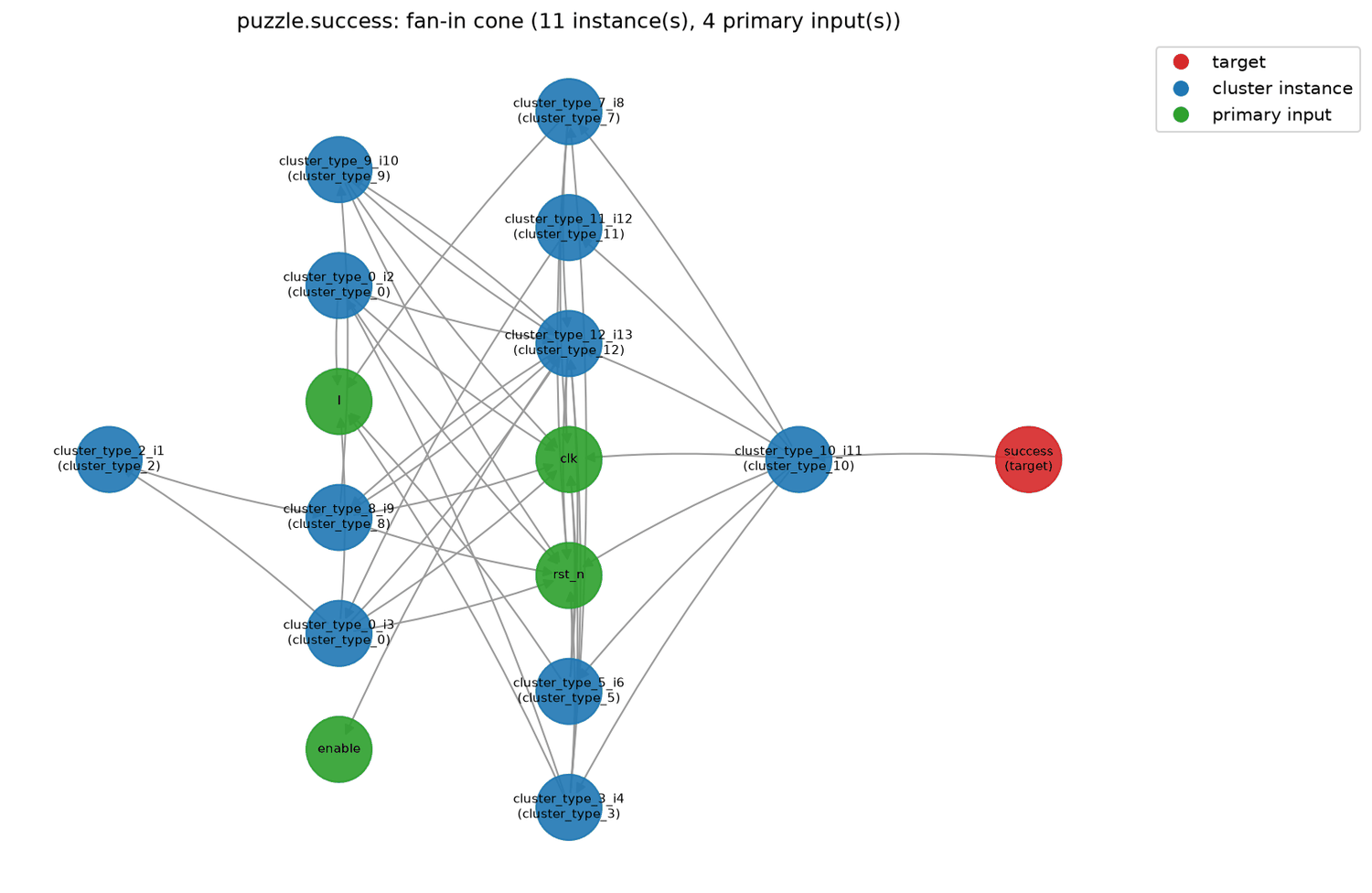
Figure 33 — Fan-in graph traced backward from success, showing every cluster instance and primary input that feeds it.
Third attempt: simulate each cluster independently in Python and build truth tables, treating each flip-flop's current state as an input and reading off its next state. That verified what I'd worked out about cluster8/cluster9 and turned up constraints between clusters. Reordering the clusters in the Verilog file also made the input flow easier to follow.
The key find: A_27 has to be armed high for success to go high, and A_27 is independent of the serial input I — it's driven purely by the cluster8/cluster9 counter. Solving for how many cycles it takes A_27 to go high gives the input length: len(I) = 121.
Once enough clusters were simulated and enough inter-cluster constraints were pinned down, I finally had enough of a chip model to build one Z3 model over the whole thing and solve for an input that drives success high. I ran it, decoded the output stream expecting a payoff — and got garbage (Figure 34).
success: True  (cycle 122)
message: 'd.@.....,.C..3.'
Figure 34 — Decoded output stream for the first success = 1 solution (not valid ASCII).
That was odd enough to be a signal, not a bug: success = 1 wasn't the whole story. I added one more constraint — force the output stream to decode as printable ASCII — and solved again.
success: True  (cycle 122)
message: '(* TWO STARS *)'
Figure 35 — With an ASCII constraint added, the output decodes to (* TWO STARS *).
This time it printed (* TWO STARS *). A star-themed message hidden behind an extra constraint was clearly not an accident.
Easter eggs
That TWO STARS message made it clear the puzzle had more going on than a single success bit.
The first easter egg had been in plain sight the whole time: the sample .vcd Jane Street provided contains the literal string "leave no stone unturned" — in hindsight, a hint that the garbage-text success = 1 solution wasn't the end.
As a sanity check I tried the simplest inputs. All 1's (Figure 36): success stays low, but the garbage decode still spells something — BBIG BANG. All 0's (Figure 37): also success = 0, decoding to EEMPTY SKY.
success: False
message: 'BBIG BANG'
Figure 36 — All-1's input: success stays low, but the decode still spells BBIG BANG.
success: False
message: 'EEMPTY SKY'
Figure 37 — All-0's input: success stays low, decoding to EEMPTY SKY.
Another easter egg was hiding in the geometry. Opening puzzle.gds in the viewer, two cells — INTERNAL_3 and INTERNAL_7 — looked invisible on the map. Inspecting them with gdstk showed they did have polygons, so I plotted every instance by position (Figure 38).

Figure 38 — Raw x-position plot of every INTERNAL_3/INTERNAL_7 instance in puzzle.gds.
Two kinds of dot in a sequence, with uneven gaps between them: Morse. Every dot was followed by a space, so I read INTERNAL_3 as dot and INTERNAL_7 as dash and re-plotted with the spacing grouped (Figure 39). It decodes to "PER ARENAM AD ASTRA" — "through sand to the stars" — a play on per aspera ad astra ("through hardship to the stars"), presumably nodding at sand → silicon.
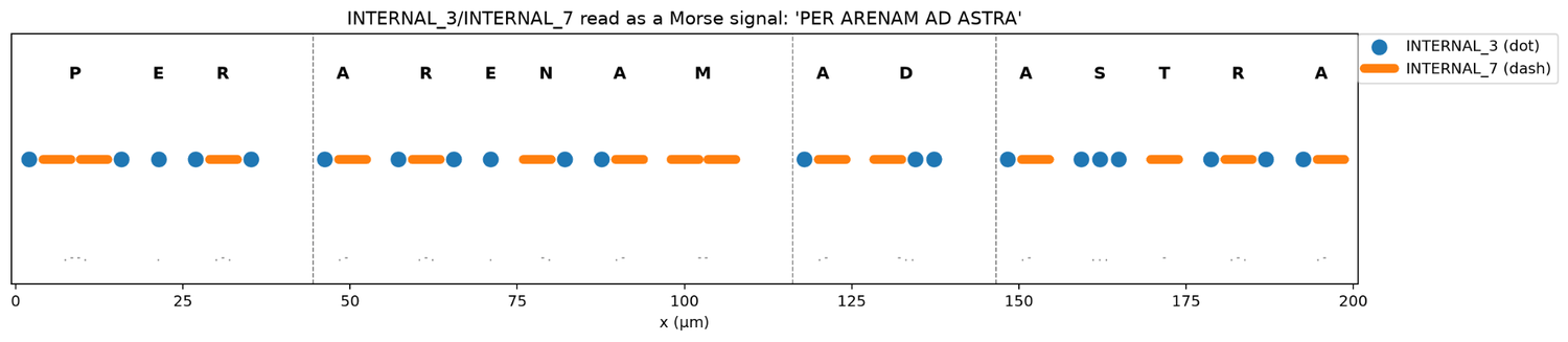
Figure 39 — Replotted with INTERNAL_3 = dot, INTERNAL_7 = dash: "PER ARENAM AD ASTRA".
An 11×11 input grid
With one easter egg decoded, I went back to the numbers — starting with the 121 that had now shown up twice. 121 is a perfect square, so I reshaped the input stream into an 11×11 grid (Figure 40). The result: every row has exactly two 1's, and so does every column. And the readable output was TWO STARS.
A friend pointed out that this looks like a variant of Star Battle (I hadn't heard of it — thestarstruckgame.com). The 11×11 made sense then: this is the two-stars-per-row-and-column variant, and the whole chip is essentially a checker for a valid solution to that puzzle — and it's looking for one specific solution.
00000100010
10000001000
00000001010
10001000000
00100010000
00100010000
00001000001
01000000100
00000000101
00010100000
01010000000
Figure 40 — The 11×11 grid for the readable solution, printed as 11 binary rows: two 1's in every row and column.
The two-per-row/two-per-column property holds for every input that drives success high, not just the readable one, so it can't be what makes one solution special — and Star Battle's "no two stars touch" rule doesn't hold for the garbage-text solution. As with adder_demo, I used Z3 to enumerate solutions, blocking each and re-solving: 16 valid inputs in total.
That points to one specific Star Battle configuration being the intended answer. The original game also constrains one star per colored region — so what are the regions here? My guess is that it's tied to the physical layout of the clusters.
I ran out of contest time before pinning that down. Recovering the region map for this two-star variant — and with it the one intended solution — is where I'd pick this back up.